Monday, 12 Jan 2026
Subscribe
logo
  • Global
  • AI
  • Cloud Computing
  • Edge Computing
  • Security
  • Investment
  • Sustainability
  • More
    • Colocation
    • Quantum Computing
    • Regulation & Policy
    • Infrastructure
    • Power & Cooling
    • Design
    • Innovations
    • Blog
Font ResizerAa
Data Center NewsData Center News
Search
  • Global
  • AI
  • Cloud Computing
  • Edge Computing
  • Security
  • Investment
  • Sustainability
  • More
    • Colocation
    • Quantum Computing
    • Regulation & Policy
    • Infrastructure
    • Power & Cooling
    • Design
    • Innovations
    • Blog
Have an existing account? Sign In
Follow US
© 2022 Foxiz News Network. Ruby Design Company. All Rights Reserved.
Data Center News > Blog > Innovations > Thick-film conductive ink suitable for large-area, large-current printed electronics
Innovations

Thick-film conductive ink suitable for large-area, large-current printed electronics

Last updated: March 3, 2024 4:33 pm
Published March 3, 2024
Share
Thick-film conductive ink suitable for large-area, large-current printed electronics
SHARE
(a) Thick-film conductive ink. (b) Versatile substrate with patterns printed on its floor utilizing the thick-film conductive ink. (c) Number of steel advanced inks which can be used to synthesize the thick-film conductive ink. (d) Copper particles. Credit score: Nationwide Institute for Supplies Science

A thick-film, electrically conductive ink appropriate for printing digital circuits and sensors on the surfaces of movies and different substrates to fabricate printed electronics has been collectively developed by NIMS, Sumitomo Steel Mining Co., Ltd. (primarily based in Minato Metropolis, Tokyo), N.E. CHEMCAT CORPORATION (primarily based in Minato Metropolis, Tokyo) and Priways Co., Ltd. (a NIMS-founded startup primarily based in Tsukuba, Ibaraki).

Printed electronics are manufactured utilizing additive strategies (i.e., digital circuits are immediately printed on the surfaces of substrates) relatively than typical subtractive electronics manufacturing (i.e., metallic movies are first deposited on substrate surfaces and pointless movie areas are then eliminated to kind circuits).

The additive methodology makes use of much less metallic supplies than the subtractive methodology, making it extra environmentally pleasant and cheap. As well as, the additive methodology can be utilized to print digital circuits on the surfaces not solely of inflexible substrates but additionally versatile ones. Due to these benefits, the additive methodology is anticipated to function an efficient wiring approach to be used in next-generation gadget fabrication.

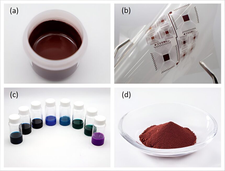
The brand new thick-film conductive ink was created utilizing steel advanced inks (i.e., inks consisting of a central metallic ion surrounded by charged molecular ligands) developed by NIMS and Priways and metallic powder synthesis and paste manufacturing applied sciences developed by Sumitomo Steel Mining.

This ink is ready to meet printed electronics necessities: its thickness is controllable and it’s suitable with low-temperature sintering. These enhancements had been achieved by including copper particles developed by Sumitomo Steel Mining to the ink, enabling it to kind thick-film wiring at about 200°C on the surfaces of heat-resistant plastic movies.

See also  Scalable method creates self-healing, stretchable transistors and circuits

The main points of the know-how have been published within the journal Utilized Floor Science.

The newly developed ink is extra cheap to synthesize and extra oxidation-resistant than typical conductive inks. As well as, the thickness of the ink movie might be greater than 3 times bigger than that of typical ink movies, making it appropriate to be used in large-current, large-area digital merchandise.

The analysis staff is presently growing strategies for mass-producing this ink by leveraging N.E. CHEMCAT’s experience in steel advanced improvement and manufacturing. The staff plans to additional enhance the efficiency of the ink and establish different purposes for it.

Extra info:
Wanli Li et al, Printing versatile Cu–Ni traces with excessive conductivity and excessive thermal stability by in-situ shaped multiscale core–shell constructions in inks, Utilized Floor Science (2023). DOI: 10.1016/j.apsusc.2023.158967

Supplied by
Nationwide Institute for Supplies Science


Quotation:
Thick-film conductive ink appropriate for large-area, large-current printed electronics (2024, February 27)
retrieved 3 March 2024
from https://techxplore.com/information/2024-02-thick-ink-suitable-large-area.html

This doc is topic to copyright. Aside from any truthful dealing for the aim of personal research or analysis, no
half could also be reproduced with out the written permission. The content material is supplied for info functions solely.


Source link

TAGGED: conductive, electronics, ink, largearea, largecurrent, printed, suitable, Thickfilm
Share This Article
Twitter Email Copy Link Print
Previous Article Bitcoin Dogs ICO Raises $5.7 Million, Pioneering BRC-20 and Bitcoin Gaming Bitcoin Dogs ICO Raises $5.7 Million, Pioneering BRC-20 and Bitcoin Gaming
Next Article SciTechDaily Unlocking the Universe’s Oldest Mysteries With Webb
Leave a comment

Leave a Reply Cancel reply

Your email address will not be published. Required fields are marked *

Your Trusted Source for Accurate and Timely Updates!

Our commitment to accuracy, impartiality, and delivering breaking news as it happens has earned us the trust of a vast audience. Stay ahead with real-time updates on the latest events, trends.
FacebookLike
TwitterFollow
InstagramFollow
YoutubeSubscribe
LinkedInFollow
MediumFollow
- Advertisement -
Ad image

Popular Posts

AWS offers a glimpse of its AI networking infrastructure

For instance, AWS lately delivered a brand new community optimized for generative AI workloads –…

July 16, 2024

DuckDuckGo launches $9.99 per month privacy bundle with VPN

DuckDuckGo is saying a brand new bundled subscription service, Privateness Professional, that provides a further…

April 11, 2024

Robotics meets the culinary arts

The edible robotic cake is the results of a collaboration between researchers from EPFL (the…

April 20, 2025

Shadow AI is consulting’s survival strategy in the GenAI era

Be part of our every day and weekly newsletters for the newest updates and unique…

May 27, 2025

Connectivity Wireless Raises $200M

Connectivity Wireless, a Boca Raton, FL-based supplier of in-building wi-fi options, acquired $200M. The quantity…

March 30, 2025

You Might Also Like

6G
Innovations

Anritsu and VTT push boundaries of D-band wireless communications

By saad
Laser breakthrough brings 2D materials closer to chip factories
Innovations

Laser breakthrough brings 2D materials closer to chip factories

By saad
SHASAI project to protect AI systems against cybersecurity threats
Innovations

SHASAI project to protect AI systems against cybersecurity threats

By saad
Join the EUPEX workshop on ARM-based architectures at HiPEAC 2026
Innovations

Join the EUPEX workshop on ARM-based architectures at HiPEAC 2026

By saad
Data Center News
Facebook Twitter Youtube Instagram Linkedin

About US

Data Center News: Stay informed on the pulse of data centers. Latest updates, tech trends, and industry insights—all in one place. Elevate your data infrastructure knowledge.

Top Categories
  • Global Market
  • Infrastructure
  • Innovations
  • Investments
Usefull Links
  • Home
  • Contact
  • Privacy Policy
  • Terms & Conditions

© 2024 – datacenternews.tech – All rights reserved

Welcome Back!

Sign in to your account

Lost your password?
We use cookies to ensure that we give you the best experience on our website. If you continue to use this site we will assume that you are happy with it.
You can revoke your consent any time using the Revoke consent button.