Gallium nitride-based semiconductors have been a boon for high-frequency and energy electronics. They’ve additionally revolutionized energy-efficient LED lighting. However no semiconductor wafer has been capable of do each on the similar time effectively.
Now Cornell researchers, in collaboration with a workforce on the Polish Academy of Sciences, have developed the primary dual-sided—or “dualtronic”—chip that mixes its photonic and digital features concurrently, an innovation that might shrink the dimensions of practical gadgets, make them extra power environment friendly and scale back manufacturing prices.
The workforce’s paper, “Using Both Faces of Polar Semiconductor Wafers for Functional Devices,” printed Sept. 25 in Nature. The co-lead authors are doctoral college students Len van Deurzen and Eungkyun Kim.
The undertaking was led by Debdeep Jena, the David E. Burr Professor of Engineering within the Faculty of Electrical and Laptop Engineering and Division of Supplies Science and Engineering, and Huili Grace Xing, the William L. Quackenbush Professor of Electrical and Laptop Engineering and of Supplies Science and Engineering, each in Cornell Engineering.
Gallium nitride (GaN) is exclusive amongst wide-bandgap semiconductors as a result of it has a big digital polarization alongside its crystal axis, which supplies every of its surfaces dramatically completely different bodily and chemical properties. The gallium, or cation, facet has proved helpful for photonic gadgets akin to LEDs and lasers, whereas the nitrogen, or anion, facet can host transistors.
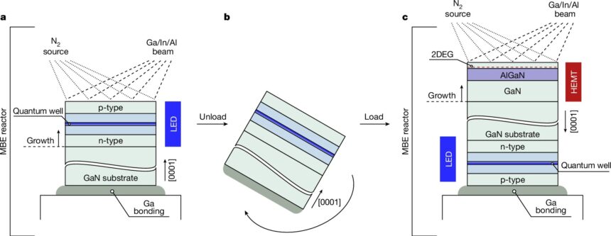
The Jena-Xing Laboratory got down to make a practical machine by which a excessive electron mobility transistor (HEMT) on one facet drives light-emitting diodes (LEDs) on the opposite—a feat that hasn’t been achieved in any materials.
“To our information, no person has made energetic gadgets on each side, not even for silicon,” van Deurzen mentioned. “One of many causes is that there is not any extra performance you get from utilizing each side of a silicon wafer as a result of it is cubic; each side are principally the identical. However gallium nitride is a polar crystal, so one facet has completely different bodily and chemical properties than the opposite, which supplies us further diploma in designing gadgets.”
The undertaking was initially conceived at Cornell by Jena and former postdoctoral researcher Henryk Turski, a co-senior writer of the paper, together with Jena and Xing. Turski labored with a workforce on the Polish Academy of Sciences’ Institute of Excessive Strain Physics to develop clear GaN substrates on a single crystal wafer roughly 400 microns thick.
The HEMT and LED heterostructures had been then grown in Poland by molecular beam epitaxy. After the epitaxy was accomplished, the chip was shipped to Cornell, the place Kim constructed and processed the HEMT on the nitrogen polar face.
“The nitrogen polar facet is extra chemically reactive, which implies throughout machine processing the electron channel could be broken fairly simply,” Kim mentioned. “A problem with nitrogen polar transistor fabrication is to verify all of the plasma processes and the chemical therapy don’t harm the transistors. So there was lots of course of improvement that needed to be performed for fabricating and designing that transistor.”
Subsequent, van Deurzen constructed the LED on the metallic polar face, utilizing a thick optimistic picture resist coating to guard the beforehand processed n-polar face. After every stage, the researchers measured their respective machine traits and located they’d not modified.
“It is truly a really possible course of,” van Deurzen mentioned. “The gadgets don’t degrade. And that is clearly vital if you wish to use this as an actual know-how.”
Since nobody has made a double-sided semiconductor machine earlier than, the workforce needed to invent a brand new methodology to check and measure it. They assembled a “crude” double-side-coated glass plate and wire-bonded one facet of the wafer to it, which allowed them to probe each side from the highest.
As a result of the GaN substrates had been clear for the whole seen vary, the sunshine was capable of transmit by way of. The one HEMT machine succeeded in driving a big LED, turning it on and off at kilohertz frequencies—loads for a working LED show.
Presently, LED shows have a separate transistor and unbiased fabrication processes. A right away software for the dualtronic chip is microLEDs: fewer parts, occupying a smaller footprint and requiring much less power and supplies, and manufactured faster for decrease price.
“A very good analogy is the iPhone,” Jena mentioned. “It’s, in fact, a telephone, however it’s so many different issues. It is a calculator, it is a map, it permits you to test the web. So there is a little bit of a convergence side of it. I might say our first demonstration of ‘dualtronics’ on this paper is convergence of perhaps two or three functionalities, however actually it is greater than that.
“Now you could not require the completely different processors to carry out completely different features, and scale back the power and pace misplaced within the interconnections between them that requires additional electronics and logic. A lot of these functionalities shrink into one wafer with this demonstration.”
Different purposes embody Complementary Steel-Oxide-Semiconductor (CMOS) gadgets with a polarization-induced n-channel transistor (which makes use of electrons) on one facet and a p-channel transistor (containing holes) on the opposite.
As well as, as a result of the GaN substrates have a excessive piezoelectric coefficient, they can be utilized as bulk acoustic wave resonators for filtering and amplifying radio frequency indicators in 5G and 6G communications. The semiconductors might additionally incorporate lasers as a substitute of LEDs for “LiFi”—i.e., light-based—transmissions.
“You may basically prolong this to allow the convergence of photonic, digital and acoustic gadgets,” van Deurzen mentioned. “You are basically restricted by your creativeness by way of what you would do, and unexplored functionalities can emerge once we strive them sooner or later.”
Extra data:
Len van Deurzen, Utilizing each faces of polar semiconductor wafers for practical gadgets, Nature (2024). DOI: 10.1038/s41586-024-07983-z. www.nature.com/articles/s41586-024-07983-z
Quotation:
There’s two sides to this semiconductor, and plenty of simultaneous features (2024, September 25)
retrieved 25 September 2024
from https://techxplore.com/information/2024-09-sides-semiconductor-simultaneous-functions.html
This doc is topic to copyright. Other than any honest dealing for the aim of personal examine or analysis, no
half could also be reproduced with out the written permission. The content material is supplied for data functions solely.