Silicon semiconductors utilized in present photodetectors have low mild responsivity, and the two-dimensional semiconductor MoS₂ (molybdenum disulfide) is so skinny that doping processes to manage its electrical properties are tough, limiting the belief of high-performance photodetectors.
A KAIST analysis crew has overcome this technical limitation and developed the world’s highest-performing self-powered photodetector, which operates with out electrical energy in environments with a lightweight supply. This paves the way in which for exact sensing with out batteries in wearable units, biosignal monitoring, IoT units, autonomous autos, and robots, so long as a lightweight supply is current.
Professor Kayoung Lee’s analysis crew from the College of Electrical Engineering developed the self-powered photodetector, which demonstrated a sensitivity as much as 20 occasions greater than present merchandise, marking the best efficiency stage amongst comparable applied sciences reported so far. The work is published within the journal Superior Useful Supplies.
The crew fabricated a PN junction construction photodetector able to producing electrical alerts by itself in environments with mild, even with out {an electrical} power provide, by introducing a “van der Waals backside electrode” that makes semiconductors extraordinarily delicate to electrical alerts with out doping.
A PN junction is a construction fashioned by becoming a member of p-type (hole-rich) and n-type (electron-rich) supplies in a semiconductor. This construction causes present to movement in a single course when uncovered to mild, making it a key element in photodetectors and photo voltaic cells.
Usually, to create a correct PN junction, a course of referred to as doping is required, which entails intentionally introducing impurities into the semiconductor to change its electrical properties. Nevertheless, two-dimensional semiconductors reminiscent of MoS₂ are just a few atoms thick, so doping within the standard means can harm the construction or cut back efficiency, making it tough to create a great PN junction.
. DOI: 10.1002/adfm.202510113")
To beat these limitations and maximize system efficiency, the analysis crew designed a brand new system construction incorporating two key applied sciences: the van der Waals electrode and the partial gate.
The partial gate construction applies {an electrical} sign solely to a part of the two-dimensional semiconductor, controlling one aspect to behave like p-type and the opposite like n-type. This permits the system to perform electrically like a PN junction with out doping.
Moreover, contemplating that standard metallic electrodes can chemically bond strongly to the semiconductor and harm its lattice construction, the van der Waals backside electrode was connected gently utilizing van der Waals forces. This preserved the unique construction of the two-dimensional semiconductor whereas guaranteeing efficient electrical sign switch.
This strategy secured each structural stability and electrical efficiency, enabling the belief of a PN junction in skinny two-dimensional semiconductors with out damaging their construction.
")
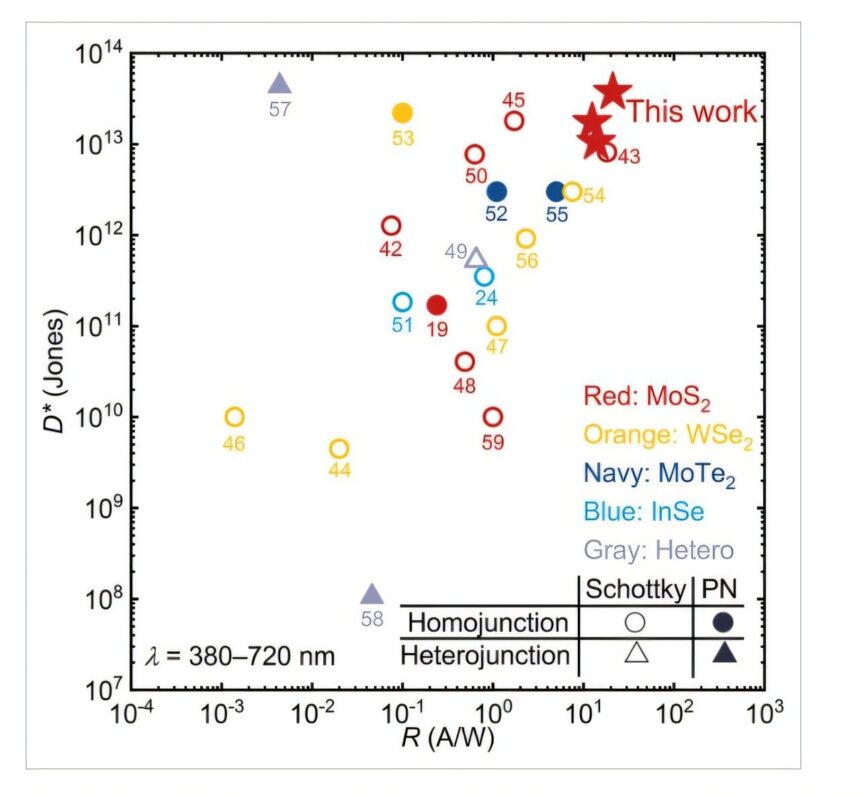
Due to this innovation, the crew succeeded in implementing a high-performance PN junction with out doping. The system can generate electrical alerts with excessive sensitivity so long as there may be mild, even with out an exterior energy supply. Its mild detection sensitivity (responsivity) exceeds 21 A/W, greater than 20 occasions greater than powered standard sensors, 10 occasions greater than silicon-based self-powered sensors, and greater than twice as excessive as present MoS₂ sensors. This stage of sensitivity means it may be utilized instantly to high-precision sensors able to detecting biosignals or working in darkish environments.
Professor Kayoung Lee mentioned that they’d “achieved a stage of sensitivity unimaginable in silicon sensors, and though two-dimensional semiconductors are too skinny for standard doping processes, [they] succeeded in implementing a PN junction that controls electrical movement with out doping.”
“This know-how can be utilized not solely in sensors, but in addition in key parts that management electrical energy inside smartphones and digital units, offering a basis for miniaturization and self-powered operation of next-generation electronics,” added Professor Lee.
Extra info:
Jaeha Hwang et al, Gated PN Junction in Ambipolar MoS2 for Superior Self‐Powered Photodetection, Superior Useful Supplies (2025). DOI: 10.1002/adfm.202510113
Quotation:
Self-powered photodetector achieves 20-fold sensitivity increase utilizing novel system construction (2025, August 18)
retrieved 18 August 2025
from https://techxplore.com/information/2025-08-powered-photodetector-sensitivity-boost-device.html
This doc is topic to copyright. Aside from any truthful dealing for the aim of personal research or analysis, no
half could also be reproduced with out the written permission. The content material is offered for info functions solely.