Kvanttinova’s CEO, Jussi Tuovinen, explains how Finland is remodeling its expertise ecosystem to develop into a worldwide chief in chip improvement.
The very important function of crucial expertise has been recognised worldwide. Amongst these crucial applied sciences are semiconductors and microelectronics, or, briefly, chips. The European Union declared its stand by the Chips Act in 2022.
Finland excels in specialised manufacturing and integration processes, in addition to in advanced system-on-chip design. Each have been nurtured by intimate interplay between tutorial analysis, utilized analysis and the business’s efforts to develop the analysis outcomes into flourishing enterprise.
From our perspective, synthetic intelligence (AI) is a serious driver for brand new semiconductor circuits and their energy effectivity. One other space for circuits is 6G telecommunication networks for resilient connectivity and sensing communication. A part of that is, for instance, antenna beam-steering capacities. Well being and medical fields are additionally necessary development areas for us, along with defence and area functions. Throughout latest years, newcomer expertise has stormed to public consciousness: quantum expertise for unseen prospects for computing and sensing. For us, quantum expertise has been a part of our RDI and industrial portfolio for over three a long time.
The Finnish semiconductor business presently employs roughly 7,000 specialists with a mixed income of €2bn. By 2035, the business goals to greater than triple these numbers. The businesses cowl the entire industrial worth chain and their predominant buyer segments are in telecommunication, automotive, industrial automation, and well being applied sciences.
Kvanttinova: R&D hub for microelectronics and quantum expertise
To proceed Finnish progress, help development objectives, and construct on the prevailing robust basis, we current Kvanttinova – an ecosystem for the way forward for chips and techniques, catalysing improvements and having enjoyable whereas doing it. It’s a distinctive surroundings providing new product analysis and improvement, from design to proof-of-concept validation and, moreover, pilot strains for small- to mid-volume manufacturing in 200mm and 300mm wafer sizes, i.e. scaling-up from labs to fabs. Revolutionary circuit design and superior supplies are introduced collectively in Kvanttinova to create novel new gadgets and merchandise. Utility fields for Kvanttinova applied sciences are, for instance, 6G, well being and medical, aerospace and defence, in addition to AI and quantum computing.
Jussi Tuovinen, CEO of Kvanttinova, mentioned: “Along with our associate community, we’re constructing an excellent stronger collaboration between analysis and business, encouraging important R&D and design web site investments, and even attracting investments in manufacturing websites. A shining ecosystem means prospering companies and an unlimited variety of new jobs.”
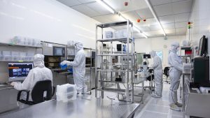
Kvanttinova. State-of-the-art beam forming FD-SOI receiver chip for
sensing functions in collaboration with Aalto College, Tampere
College and Saab is proven on this photograph. (IEEE Entry, vol. 10, pp.
116375-116383, 2022)
Kvanttinova originates domestically from Otaniemi in Espoo, with world impression and outreach.
Progress is a collaborative effort
Kvanttinova is a collaborative effort by VTT Technical Research Centre of Finland, Aalto University, Metropolis of Espoo, Enter Espoo, and the Finnish semiconductor business. It’s right here to open prospects for worldwide specialists, corporations, and investments.
Aalto College is a multifaceted larger schooling and analysis powerhouse. VTT has robust experience within the specialised microelectronics processes and quantum expertise. Significantly noteworthy is VTT’s experience in establishing and main nationwide and worldwide collaborative tasks, bringing collectively analysis and business wants. Espoo’s innovation ecosystem helps the expansion of small and huge corporations by connecting investments and companions to the ecosystem.
Kvanttinova builds on Micronova, a longtime RDI hub that’s well-known within the Finnish microelectronics neighborhood. The mannequin is already in place with tutorial and utilized analysis co-located along with the economic presence. The Micronova cleanroom is utilized by Aalto College and VTT, that are joined by a number of corporations performing improvement and even manufacturing operations there.
Espoo innovation neighborhood accelerates success
We’ve got our distinctive recipe and now we’re scaling up. As an alternative of a single cleanroom the place corporations utilise Aalto College or VTT-owned gear, we give corporations the chance to have their very own cleanrooms, massive or small. The cleanrooms are related internally to the shared-use amenities, thus permitting corporations to combine their operations seamlessly into a bigger infrastructure.
Micronova RDI hub has been a vibrant springboard to a bunch of fascinating, groundbreaking expertise corporations, equivalent to IQM and SemiQon, and attracted corporations to additional develop their improvements within the neighborhood, equivalent to Dispelix. The multi-user semiconductor piloting surroundings in Micronova helps the processing of various applied sciences together with micro-electromechanical techniques (MEMS) and microoptoelectromechanical techniques (MOEMS), quantum gadgets, radio frequency (RF) elements, built-in photonics gadgets, and 2D supplies and post-CMOS processed elements.
Espoo’s innovation neighborhood in Finland provides globally main quantum expertise and semiconductor experience, abilities, and infrastructure – and will probably be one among Europe’s important quantum and semiconductor business hubs sooner or later.
IQM Quantum Computer systems: A worldwide chief in superconducting quantum computer systems
Hop on the sunshine rail tram in Espoo, and you’ll be rapidly transported to maybe the world’s most concentrated space of quantum expertise experience. Inside a few tram stops, you may attain lots of Finland’s main quantum gamers. Certainly one of these is IQM Quantum Computer systems (IQM) – a worldwide chief in superconducting quantum computer systems.
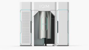
IQM was based in 2018, because it spun out of VTT and Aalto College. Now, the corporate has its personal quantum pc fabrication facility, design, software program, and one of many largest quantum engineering groups on the planet. IQM designs, builds, and sells on-premises full-stack quantum computer systems. IQM additionally offers a cloud platform for patrons to entry its computer systems wherever on the planet.
Like many different VTT and Aalto spin-offs, IQM has embraced its robust ties to Espoo’s open innovation neighborhood. Along with VTT, IQM launched Finland’s first quantum pc in 2021. In 2023, they unveiled the 20-qubit quantum system. Now, the 2 are constructing a 50-qubit pc set to be launched later in 2025.
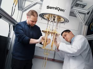
SemiQon: Serving to to make future quantum computer systems extra reasonably priced, scalable and sustainable
Primarily based in Espoo with roots in Micronova, SemiQon helps to develop silicon-based quantum processors to make future quantum computer systems extra reasonably priced, scalable, and sustainable. The startup spun out of VTT in early 2023.
SemiQon’s expertise builds upon a long time of improvement and knowhow from the semiconductor business, making their silicon processors commercially aggressive and well-suited for mass manufacturing. The corporate believes that the wedding of quantum and semiconductors not solely scales up quantum computing successfully but additionally boosts manufacturing, builds resilience, and helps technological sovereignty. The help from the native quantum and enterprise ecosystem has been pivotal for the corporate’s success.
Dispelix: Finnish augmented actuality (AR) pioneer on the forefront of the fast-evolving waveguide show market
Espoo’s collaborative innovation actuality offers the right surroundings for tech improvement. One of many high-tech builders on this ecosystem is Dispelix, a Finnish augmented actuality (AR) pioneer headquartered in Espoo. Dispelix is remodeling the way forward for AR by its clear show expertise, waveguides, that are used as see-through shows in varied AR functions. Dispelix show expertise may be utilized to, for instance, near-eye shows for good glasses and headsets, in addition to to head-up shows in automobiles and aviation.
For a high-tech firm like Dispelix, Espoo’s innovation ecosystem – with its collaborative working tradition, worldwide ambiance, and amenities like the most important cleanroom within the Nordics at Micronova – provides an open and supportive surroundings for achievement.
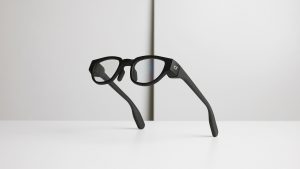
Dispelix’s pioneering expertise is backed by an in depth IP portfolio and expert personnel of roughly 100 gifted staff. Final yr, Dispelix celebrated recording its two hundredth patent within the books for waveguide show expertise. As we speak, this quantity has grown to over 230, with greater than 230 extra patent functions pending. These sorts of milestones are becoming for a science-driven firm positioned within the coronary heart of Espoo’s innovation ecosystem, the place the innovation gamers utilized for the sixth most patents in Europe and made 60.5% of all Finnish patent functions final yr.
Reinventing the ecosystem – and having enjoyable whereas doing it
The core of the Kvanttinova infrastructure is the shared-use facility which hosts state-of-the-art gear for chip improvement and pilot manufacturing on 200mm and 300mm wafers, providing main advantages in improved reliability and repeatability of the processes. The gear is a part of the Chips JU (Joint Enterprise) pilot strains specializing in absolutely depleted silicon on insulator (FD-SOI) expertise (FAMES), heterogeneous system integration and meeting (APECS), sub 2nm system-on-chip (SoC) expertise (NanoIC), and photonic built-in circuits (PIXEurope).
The ability provides particular capabilities in materials improvement for things like ferro- and piezoelectric supplies, integration and packaging, superconducting and RF elements, and built-in photonics. These piloting strains allow the technology of concepts and their scaling with minimal personal capital for the beginning entrepreneur.
As necessary as this fascinating new facility and infrastructure is, we’re much more excited to facilitate our neighborhood, outdated and new pals, to fulfill, to study and to co-create, resulting in development for us all. A widely known truth is that collectively we’re stronger. Collectively we will even have our cake and eat it too. Kvanttinova will develop to a number one semiconductor hub for innovation, offering an surroundings and help to scale science-based improvements to enterprise.
Kvanttinova welcomes all facets of microelectronics right into a single neighborhood. It’s a hotspot for encounters and co-creation. We need to obtain a sense of togetherness among the many completely different actors in our neighborhood by working throughout the RDI hub, attending varied occasions and co-creating organized, and even random encounters.
Kvanttinova co-operates with instructional institutes of all ranges to seek out solutions to the frequent problem of the place to get the abilities and expertise to realize the formidable targets of the semiconductor business. We’re decided to work laborious to advertise the sphere to potential college students, ranging from the early years to persuade the youth of the significance of microelectronics, chips, and techniques. By participating the scholars already of their research, we will guarantee them of a flourishing future and strengthen their understanding of potential careers. Going even deeper, we intention to help the tutorial establishments in outlining novel instructional ideas for up- and re-skilling of present workforce.
We strongly imagine sustainable chip expertise results in vitality and competitiveness of any industrial vertical trying to enhance their digitalisation degree by integrating chips and techniques into their merchandise and choices. Selling the advantages whereas elevating consciousness of the supply of providers for the design and processing of chips will deliver new customers and clients to providers and corporations producing chips and techniques.
Kvanttinova can help find R&D consortia and funding by its connections. Along with the companions within the Finnish Chips Competence Middle (FiCCC), we will deliver pilot strains, design centres, and European-level networks of competence nearer to all who collaborate with us.
We welcome all events to collaborate with our ecosystem, Kvanttinova.
Please observe, this text may even seem within the twenty first version of our quarterly publication.