Not like historically printed circuit boards, that are flat, 3D circuitry permits parts to be stacked and built-in vertically—dramatically lowering the footprint required for gadgets.
Advancing the frontiers of 3D printed circuits, a workforce of researchers from the Nationwide College of Singapore (NUS) has developed a state-of-the-art method—generally known as tension-driven CHARM3D—to manufacture three-dimensional (3D), self-healing digital circuits. This new method permits the 3D printing of free-standing metallic buildings with out requiring help supplies and exterior strain.
The analysis workforce led by Affiliate Professor Benjamin Tee from the Division of Supplies Science and Engineering within the NUS Faculty of Design and Engineering used Area’s metallic to display how CHARM3D can fabricate a variety of electronics, permitting for extra compact designs in gadgets comparable to wearable sensors, wi-fi communication techniques and electromagnetic metamaterials.
In well being care, for example, CHARM3D facilitates the event of contactless important signal monitoring gadgets—enhancing affected person consolation whereas enabling steady monitoring. In sign sensing, it optimizes the efficiency of 3D antennas, resulting in improved communication techniques, extra correct medical imaging and sturdy safety purposes.
The workforce’s findings had been published within the journal Nature Electronics on 25 July 2024. Assoc Prof Tee is the corresponding creator of the analysis paper.
A extra streamlined strategy to 3D circuit manufacturing
3D digital circuits more and more underpin fashionable electronics, from battery know-how to robotics to sensors, enhancing their functionalities whereas enabling additional miniaturization. For instance, 3D architectures, with their massive efficient floor areas, enhance battery capability and improve sensor sensitivity.
Direct ink writing (DIW), a promising 3D printing method at present used to manufacture 3D circuits, poses vital drawbacks. The crux lies in its use of composite inks, which have low electrical conductivity and entail help supplies to help in solidification after printing. The inks are additionally too viscous, limiting printing pace.
Enter Area’s metallic, an eutectic alloy of indium, bismuth and tin. Eutectic alloys soften and freeze at a single temperature decrease than the melting factors of their constituent metals—providing a beautiful various materials for 3D printing. With a low melting level of 62°C, a excessive electrical conductivity and low toxicity, Area’s metallic, not like composite inks, solidifies quickly—a vital attribute that permits the printing course of to eschew help supplies and exterior strain.
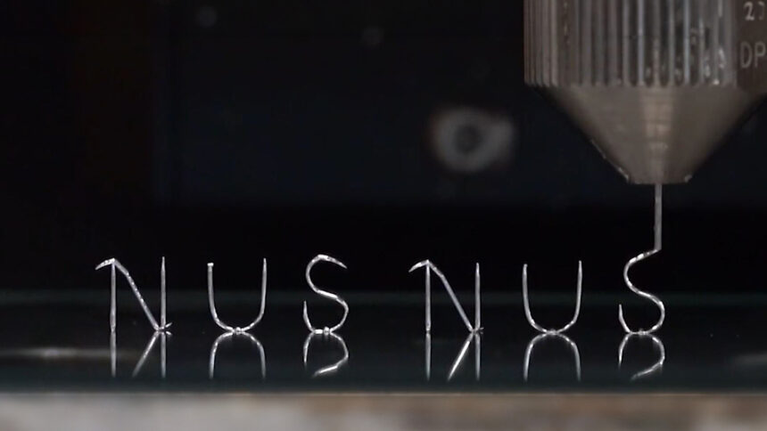
Leveraging the low melting level of Area’s metallic, the CHARM3D method exploits the stress between molten metallic in a nozzle and the forefront of the printed half, culminating in uniform, clean microwire buildings with adjustable widths of 100 to 300 microns, roughly the width of 1 to 3 strands of human hair. Critically, phenomena comparable to beading and uneven surfaces—attribute of pressure-driven DIW—are additionally absent in CHARM3D.
In comparison with standard DIW, CHARM3D provides sooner printing speeds of as much as 100 millimeters per second and better resolutions, providing a better stage of element and accuracy in circuit fabrication. CHARM3D forgoes post-treatment steps and permits the fabrication of complicated free-standing 3D buildings, comparable to vertical letters, cubic frameworks and scalable helixes. Furthermore, these 3D architectures exhibit glorious structural retention with self-healing capabilities, which means they will mechanically recuperate from mechanical injury and are recyclable.
“By providing a sooner and easier strategy to 3D metallic printing as an answer for superior digital circuit manufacturing, CHARM3D holds immense promise for the industrial-scale manufacturing and widespread adoption of intricate 3D digital circuits,” stated Assoc Prof Tee.

Far-reaching purposes
The researchers efficiently printed a 3D circuit for wearable battery-free temperature sensors, antennas for wi-fi important signal monitoring and metamaterials for electromagnetic wave manipulation—capturing the variety of purposes enabled by CHARM3D.
Conventional hospital tools comparable to electrocardiograms and pulse oximeters require pores and skin contact, which may trigger discomfort and danger infections. By CHARM3D, contact-free sensors will be built-in into sensible clothes and antennas, offering steady, correct well being monitoring in hospitals, assisted-living amenities or residence settings.
Moreover, arrays of 3D antennas or electromagnetic metamaterial sensors—fabricated through CHARM3D—may optimize sign sensing and processing purposes. This results in improved signal-to-noise ratios and better bandwidths. The method opens up the potential for creating specialised antennas for focused communication, enabling extra correct medical imaging, comparable to microwave breast imaging for early tumor detection, and superior safety purposes, comparable to detecting hidden gadgets or contraband emitting particular electromagnetic signatures.
Different collaborators on this work embrace Dr. Zhuangjian Liu from Company for Science, Expertise and Analysis’s Institute of Excessive Efficiency Computing and Professor Michael Dickey from North Carolina State College’s Division of Chemical and Biomolecular Engineering.
Subsequent steps
The analysis workforce envisions that this system will be prolonged to different kinds of metals and structural purposes. The workforce can also be in search of alternatives to commercialize this distinctive strategy to metallic printing.
Extra data:
Shaohua Ling et al, Stress-driven three-dimensional printing of free-standing Area’s metallic buildings, Nature Electronics (2024). DOI: 10.1038/s41928-024-01207-y
Quotation:
Novel method to manufacture three-dimensional circuits for superior electronics (2024, July 29)
retrieved 1 August 2024
from https://techxplore.com/information/2024-07-technique-fabricate-dimensional-circuits-advanced.html
This doc is topic to copyright. Aside from any honest dealing for the aim of personal research or analysis, no
half could also be reproduced with out the written permission. The content material is offered for data functions solely.