Monday, 12 Jan 2026
Subscribe
logo
  • Global
  • AI
  • Cloud Computing
  • Edge Computing
  • Security
  • Investment
  • Sustainability
  • More
    • Colocation
    • Quantum Computing
    • Regulation & Policy
    • Infrastructure
    • Power & Cooling
    • Design
    • Innovations
    • Blog
Font ResizerAa
Data Center NewsData Center News
Search
  • Global
  • AI
  • Cloud Computing
  • Edge Computing
  • Security
  • Investment
  • Sustainability
  • More
    • Colocation
    • Quantum Computing
    • Regulation & Policy
    • Infrastructure
    • Power & Cooling
    • Design
    • Innovations
    • Blog
Have an existing account? Sign In
Follow US
© 2022 Foxiz News Network. Ruby Design Company. All Rights Reserved.
Data Center News > Blog > Innovations > New approach reliably integrates 2D semiconductors with dielectrics
Innovations

New approach reliably integrates 2D semiconductors with dielectrics

Last updated: April 4, 2025 9:41 pm
Published April 4, 2025
Share
New approach reliably integrates 2D semiconductors with dielectrics
SHARE
Graphene FETs over 4-inch wafer and the extracted provider mobility mapping. Credit score: Nature Electronics (2025). DOI: 10.1038/s41928-025-01353-x.

Two-dimensional (2D) semiconductor supplies may allow the event of smaller but extremely performing digital parts, thus contributing to the development of a wide range of gadgets. Whereas important strides have been made within the synthesis of 2D semiconductors with superior digital properties, their clear switch onto substrates and dependable integration in actual gadgets has to date proved difficult.

Researchers at Peking College, the Beijing Graphene Institute and different institutes in China have just lately developed a brand new methodology to combine 2D semiconductors with dielectric supplies, that are insulating supplies that assist management the circulate of electrical cost in gadgets. Their strategy, outlined in a paper published in Nature Electronics, entails the epitaxial development of an ultra-thin dielectric movie on a graphene-covered copper floor, which subsequently permits its switch onto numerous substrates with minimal defects.

“The paper emerged from recognizing persistent challenges in integrating two-dimensional supplies—similar to graphene—into microelectronic gadgets,” Zhongfan Liu, Li Lin, and Yanfeng Zhang, corresponding authors of the paper, informed Tech Xplore.

“Standard switch strategies utilizing polymer helps usually introduce chemical contamination, mechanical stress, and interfacial defects, which compromise gadget efficiency. Our examine was thus aimed toward creating a complete, wafer-scale course of that overcomes these points, by preserving graphene’s intrinsic properties and making certain a clear, well-controlled interface throughout switch and encapsulation.”

To show their newly proposed wafer-scale course of, Lin and his colleagues first synthesized a single-crystal dielectric, particularly antimony oxide (Sb2O3). They then deposited this dielectric on graphene that was grown on a Cu(111) substrate.

A new approach to reliably integrate 2D semiconductors with dielectrics
Single-crystal Sb2O3 epitaxially synthesized on graphene/Cu wafer. Credit score: Nature Electronics (2025). DOI: 10.1038/s41928-025-01353-x.

“Initially, Sb2O3 movie is epitaxially grown on the graphene through a vacuum thermal evaporation course of,” defined Lin. “The copper is then pre-treated with a water-ethanol combination to kind a skinny oxide layer, decreasing the adhesion between graphene and copper. The dielectric layer not solely helps the switch but in addition acts because the encapsulating layer, thereby defending it from contamination and mechanical injury.”

See also  New 3D printing technique integrates electronics into microchannels to create flexible, stretchable microfluidic devices

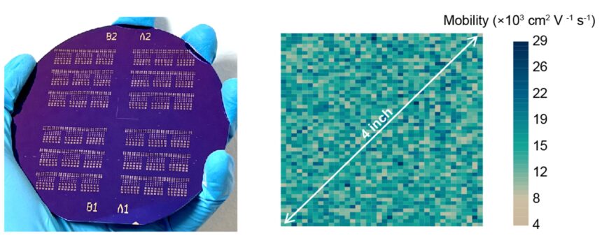
Notably, the researchers confirmed that the method enabled the dependable switch of a 4-inch graphene wafer onto goal substrates with minimal defects. Sooner or later, this might open new prospects for the event of latest electronics that mix 2D semiconductors with dielectric supplies.

“We realized the intact switch of a 4‑inch graphene wafer with preserved intrinsic electrical properties (common provider mobility of round 14,000 cm2 V-1 s-1) and built-in with single-crystal dielectric Sb2O3,” mentioned Lin. “Remarkably, our methodology ensures wonderful gadget uniformity and long-term stability, with minimal efficiency fluctuations noticed even after extended air publicity.”

This current work by Lin and his colleagues has notable sensible implications, as the tactic they developed may quickly allow the scalable fabrication of assorted extremely performing and low-power microelectronics and optoelectronics based mostly on 2D supplies.

As a part of their subsequent research, the researchers plan to construct on their strategy, whereas additionally attempting to increase it to the 3D integration of 2D supplies in actual gadgets.

“We intention to develop superior switch strategies that facilitate the stacking and exact alignment of 2D supplies to kind multi-layer, three-dimensional built-in constructions,” added Lin. “This analysis will concentrate on addressing challenges associated to interlayer coupling, interface management, and patterning in 3D configurations, finally enabling the fabrication of high-performance, densely built-in digital and optoelectronic gadgets.”

Extra info:
Junhao Liao et al, Dielectric-assisted switch utilizing single-crystal antimony oxide for two-dimensional materials gadgets, Nature Electronics (2025). DOI: 10.1038/s41928-025-01353-x.

© 2025 Science X Community

See also  Taking a hybrid approach to data centre cooling

Quotation:
New strategy reliably integrates 2D semiconductors with dielectrics (2025, April 4)
retrieved 4 April 2025
from https://techxplore.com/information/2025-04-approach-reliably-2nd-semiconductors-dielectrics.html

This doc is topic to copyright. Aside from any truthful dealing for the aim of personal examine or analysis, no
half could also be reproduced with out the written permission. The content material is supplied for info functions solely.


Source link

TAGGED: approach, dielectrics, integrates, reliably, semiconductors
Share This Article
Twitter Email Copy Link Print
Previous Article Blackstone to Buy Australia’s AirTrunk in $16B Deal Blackstone Is Said to Mull Sale of Two AirTrunk Data Centers
Next Article UK Plots 500 MW AI Cluster – But Can the Grid Keep Up? UK Plots 500 MW AI Cluster – But Can the Grid Keep Up?
Leave a comment

Leave a Reply Cancel reply

Your email address will not be published. Required fields are marked *

Your Trusted Source for Accurate and Timely Updates!

Our commitment to accuracy, impartiality, and delivering breaking news as it happens has earned us the trust of a vast audience. Stay ahead with real-time updates on the latest events, trends.
FacebookLike
TwitterFollow
InstagramFollow
YoutubeSubscribe
LinkedInFollow
MediumFollow
- Advertisement -
Ad image

Popular Posts

Indian Luxury Homebuilder to Expand into Data Centers

(Bloomberg) -- Indian property developer Rustomjee plans to construct knowledge facilities in Mumbai, the nation’s…

September 4, 2024

It’s Time to Learn about Virtual Machines! (Kali Linux VM, Windows, Ubuntu)

Digital machines are revolutionizing the best way people and companies alike strategy computing, providing unparalleled…

May 26, 2024

Microsoft to invest 2.2 billion euros in Spain data centers

FILE – The emblem of Microsoft is seen exterior its French headquarters in Issy-les-Moulineaux, exterior…

July 8, 2024

Microsoft Copilot gets 12 big updates for fall, including new AI assistant character Mico

Microsoft right this moment held a live announcement event online for its Copilot AI digital…

October 24, 2025

Modular data centres built for the AI era

The race to construct knowledge centres to assist AI and high-density computing necessities is on,…

September 24, 2025

You Might Also Like

6G
Innovations

Anritsu and VTT push boundaries of D-band wireless communications

By saad
Laser breakthrough brings 2D materials closer to chip factories
Innovations

Laser breakthrough brings 2D materials closer to chip factories

By saad
SHASAI project to protect AI systems against cybersecurity threats
Innovations

SHASAI project to protect AI systems against cybersecurity threats

By saad
Join the EUPEX workshop on ARM-based architectures at HiPEAC 2026
Innovations

Join the EUPEX workshop on ARM-based architectures at HiPEAC 2026

By saad
Data Center News
Facebook Twitter Youtube Instagram Linkedin

About US

Data Center News: Stay informed on the pulse of data centers. Latest updates, tech trends, and industry insights—all in one place. Elevate your data infrastructure knowledge.

Top Categories
  • Global Market
  • Infrastructure
  • Innovations
  • Investments
Usefull Links
  • Home
  • Contact
  • Privacy Policy
  • Terms & Conditions

© 2024 – datacenternews.tech – All rights reserved

Welcome Back!

Sign in to your account

Lost your password?
We use cookies to ensure that we give you the best experience on our website. If you continue to use this site we will assume that you are happy with it.
You can revoke your consent any time using the Revoke consent button.