The NanoIC pilot line has the ambition to turn into the world’s specialised R&D pilot line on past semiconductor know-how.
With the intention to help the European Chips Act’s imaginative and prescient to bolster Europe’s management within the international semiconductor ecosystem and drive innovation in crucial markets like computing, communication, mobility, vitality, and well being. Serving as an important bridge between cutting-edge analysis and industrial functions, the NanoIC pilot line is central to consolidating Europe’s place on the forefront of semiconductor innovation and competitiveness.
To bridge the hole between analysis innovation and commercialisation within the semiconductor {industry}, a sturdy lab-to-fab conduit is crucial. The NanoIC pilot line fosters innovation in computing system architectures by maturing particular semiconductor applied sciences. The aim is to allow European corporations to additional lead in semiconductor innovation.
Particularly, the NanoIC pilot line offers a past 2nm system-on-chip (SoC) pilot line for the event and maturation of chosen advanced logic, memory, and interconnect technologies. The mission focuses on large-scale capability constructing, particularly in imec’s cleanroom in Leuven (Belgium), joint R&D, maturation of superior applied sciences in the direction of prototyping, and innovation help, offering all the semiconductor ecosystem entry to those superior applied sciences. Contributors can interact with the NanoIC pilot line in ways in which finest go well with their particular wants and innovation objectives, no matter their function within the worth chain. This may permit early insights into the rising fields and help Europe to keep up its competitiveness throughout all the semiconductor worth chain: from supplies, gear, processes and gadgets to designs and methods.
NanoIC consortium
The NanoIC pilot line mission consortium is led by imec, alongside CEA-Leti in France, Fraunhofer-Gesellschaft (FhG) in Germany, VTT Technical Analysis Heart in Finland, Tyndall Nationwide Institute in Eire, and the Heart for Floor Science and Nanotechnology of the College Politehnica of Bucharest in Romania.It’s supported by the Flemish Authorities, different collaborating states, and the Chips Joint Enterprise. All companions collectively try to make the implementation of the pilot line successful.
Constructing blocks of future compute methods
Nanosheet class of logic gadgets are anticipated to drive scaling and efficiency by three extra generations (N2, A14, A10). Complementary area impact transistor (CFET) architectures are presently projected to be launched round 2031 on the A7 node, representing a significant inflection level in CMOS machine design. Development on this area calls for in depth analysis into new supplies, course of modules, gear, and superior patterning capabilities, for which excessive numerical aperture excessive ultraviolet (excessive NA EUV) lithography comes into play.
Reminiscence improvements are specializing in novel magnetic recollections, extra particularly spin orbit torque-magnetic random entry reminiscence (SOT-MRAM) and embedded Dynamic Random Entry Reminiscence (eDRAM). For the latter, an alternate 2T0C configuration is developed, together with the exploration of semiconductors with broad bandgaps, akin to semiconducting oxides like indium-gallium-zinc-oxide or 2D transition steel dichalcogenides, that are thought of promising various channel supplies. In parallel, growing a 3D reminiscence platform to discover future novel reminiscence choices – to reinforce SRAM and DRAM – is crucial to handle reminiscence capability and reminiscence bandwidth challenges from new workloads.
To combine totally different dies into methods, 2nm and past superior electrical and optical interconnects are required. To additional advance electrical interconnects, 3D heterogeneous integration, like die-to-wafer (D2W) hybrid bonding strategies, shall be enabled. To electrically join dies side-by-side and allow 2.5D chiplet integration on a low-cost interposer platform, the NanoIC pilot line will goal strains underneath 2µm, providing fine-pitch redistribution layer (FP RDL) know-how based mostly on copper line and through, embedded in polymers.
The above-mentioned modern logic, reminiscence, and interconnect applied sciences, outlined at industry-relevant dimensions, are on the coronary heart of the NanoIC pilot line. Their enablement requires analysis of recent processes and supplies, calls for a tighter course of management, and depends on a flexible set of validation routes. Organising related course of modules requires funding in fully new capabilities in processing and metrology instruments. These modules are the constructing blocks for the baseline flows and are susceptible to steady enhancements, making certain maturation, rising the velocity of studying and pushing in the direction of greater TRL. Stabilised baseline flows signify R&D collaboration alternatives exemplified by supplies and gear distributors to stay on the forefront of innovation.
Decreasing the obstacles to superior chip designs with superior PDKs
To assist European designers, in academia and {industry}, to discover these findings in logic, reminiscence, and interconnect applied sciences, the NanoIC pilot line offers early entry to superior course of design kits (PDKs).
These PDKs are complete toolsets that present designers with the predictive fashions, cell libraries, and system-level integration sources, enabling correct simulation and validation of built-in circuits for superior know-how nodes. By making these hands-on kits obtainable, circuit designers can discover upcoming chip architectures, deal with complicated design challenges and help innovation in past 2nm nodes.
Particularly, the NanoIC pilot line gives two complementary PDKs: pathfinding PDKs for early design exploration in beyond-state-of-the-art lC applied sciences, and system exploration PDKs to pave the way in which for {hardware} prototyping and system-level innovation.
These PDKs are being launched all through the mission and embrace a number of variations of the N2 pathfinding PDK, together with releases in A14 and A7 logic PDKs. Reminiscence PDKs are based mostly upon the progress in eDRAM and SOT-MRAM, whereas for superior interconnect options, they are often explored by RDL, silicon interposer and D2W hybrid bonding.
Driving innovation in Europe
The NanoIC pilot line offers versatile entry to superior logic, reminiscence, and interconnect applied sciences for all the semiconductor ecosystem. Firms, analysis institutes, start-ups, and universities can collaborate in keeping with their innovation wants.
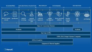
Built-in machine producers and foundries can leverage the baselines to discover new modules and efficiency enhancement choices. Tools and supplies suppliers, each European and international, are invited to collaborate to allow the superior baselines to check and refine new instruments and processes. Moreover, start-ups, universities, and design corporations have entry to the pathfinding PDK for early design exploration of future nodes and system exploration PDKs for {hardware} prototyping and system-level innovation. Furthermore, the NanoIC pilot line is dedicated to nurturing the following technology of semiconductor consultants. Partnering with the EU Competence Facilities, we offer classroom and digital programs on past 2nm applied sciences, from semiconductor supplies to SoC design. Our hands-on internships and studying programmes provide college students real-world expertise, whereas our industry-oriented trainings put together Bachelor’s, Grasp’s and PhD college students for future challenges. Via skilled programs, technical coaching, and immersive bootcamps, the NanoIC pilot line is constructing a talented workforce to propel the European semiconductor {industry} ahead.

In abstract, the NanoIC pilot line is strategically positioned to bridge the hole between cutting-edge analysis and industrial functions within the semiconductor {industry}. The mission underscores Europe’s dedication to innovation, competitiveness, and sustainable development in an more and more digital world. By advancing applied sciences and fostering collaboration, the mission goals to consolidate Europe’s management within the international semiconductor market.
Disclaimer
The acquisition and operation of the NanoIC pilot line are collectively funded by the Chips Joint Enterprise, by the European Union’s Digital Europe (101183266) and Horizon Europe programmes (101183277), in addition to by the collaborating states Belgium (Flanders), France, Germany, Finland, Eire and Romania. For extra info, go to nanoic-project.eu.
This text is predicated on the remark revealed in Nature Opinions Electrical Engineering (Quantity 1 | December 2024 | 764–765 | 764).
Please observe, this text may also seem within the twenty fourth version of our quarterly publication.