Intel has introduced a major development in built-in photonics know-how, reaching a groundbreaking milestone in high-speed information transmission. On the 2024 Optical Fiber Communication Convention (OFC), Intel‘s Built-in Photonics Options (IPS) Group showcased the {industry}’s first absolutely built-in optical compute interconnect (OCI) chiplet.
This chiplet, co-packaged with an Intel CPU, was demonstrated working dwell information, marking a considerable leap in high-bandwidth interconnect know-how for information facilities and high-performance computing (HPC) functions.
Thomas Liljeberg, Senior Director of Product Administration and Technique at IPS, highlighted the significance of this improvement, stating, “The ever-increasing motion of information from server to server is straining the capabilities of at this time’s information heart infrastructure, and present options are quickly approaching the sensible limits {of electrical} I/O efficiency. Nevertheless, Intel’s groundbreaking achievement empowers clients to seamlessly combine co-packaged silicon photonics interconnect options into next-generation compute techniques.”
The OCI chiplet is engineered to help 64 channels of 32 gigabits per second (Gbps) information transmission in every route over as much as 100 meters of fiber optics. This design goals to fulfill the escalating calls for for larger bandwidth, decrease energy consumption, and longer attain in AI infrastructure. The chiplet permits scalability of CPU/GPU cluster connectivity and helps novel compute architectures, together with coherent reminiscence enlargement and useful resource disaggregation.
Optical I/O in CPUs and GPUs
The rising deployment of AI-based functions globally, notably with developments in massive language fashions (LLMs) and generative AI, underscores the need for scalable computing platforms. These platforms require exponential progress in I/O bandwidth and prolonged attain to help bigger CPU/GPU/IPU clusters. Conventional electrical I/O options, restricted by quick attain and excessive energy consumption, have gotten insufficient for these evolving wants. Intel’s OCI chiplet, with its co-packaged xPU optical I/O answer, presents the next bandwidth, improved energy effectivity, and longer attain, addressing these vital necessities.
Utilizing an analogy, changing electrical I/O with optical I/O in CPUs and GPUs is akin to shifting from horse carriages, restricted in capability and vary, to vehicles and vehicles, able to delivering bigger portions of products over larger distances. This transition would mirror the improved efficiency and vitality effectivity that optical I/O options like Intel’s OCI chiplet carry to AI scaling.
The absolutely built-in OCI chiplet makes use of Intel’s “confirmed” silicon photonics know-how, integrating a silicon photonics built-in circuit (PIC), which incorporates on-chip lasers and optical amplifiers, with {an electrical} IC. The demonstration at OFC featured the chiplet co-packaged with an Intel CPU, nevertheless it can be built-in with future-generation CPUs, GPUs, IPUs, and different system-on-chips (SoCs).
This preliminary OCI implementation helps as much as 4 terabits per second (Tbps) bidirectional information switch, suitable with PCIe Gen5. The dwell demonstration showcased a transmitter (Tx) and receiver (Rx) connection between two CPU platforms over a single-mode fiber (SMF) patch twine. The CPUs generated and measured the optical Bit Error Charge (BER), demonstrating robust sign high quality with 8 wavelengths at 200 gigahertz (GHz) spacing on a single fiber.
The chiplet helps 64 channels of 32 Gbps information in every route over distances as much as 100 meters, although sensible functions could also be restricted to tens of meters on account of latency. It employs eight fiber pairs, every carrying eight dense wavelength division multiplexing (DWDM) wavelengths. The co-packaged answer is vitality environment friendly, consuming solely 5 pico-Joules (pJ) per bit in comparison with roughly 15 pJ/bit for pluggable optical transceiver modules. This hyper-efficiency is essential for information facilities and HPC environments, doubtlessly addressing the unsustainable energy necessities of AI infrastructure.
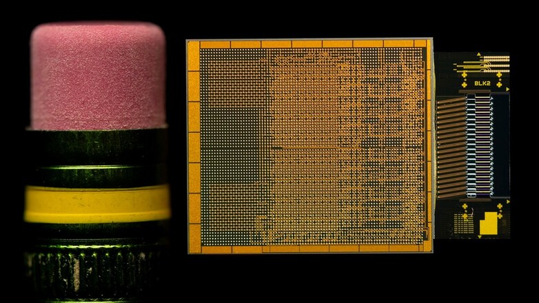
OCI Chiplet – Prototype
Intel’s management in silicon photonics is constructed on over 25 years of inner analysis, pioneering built-in photonics. The corporate says it was the primary to develop and ship silicon photonics-based connectivity merchandise with industry-leading reliability at excessive quantity to main cloud service suppliers. Intel’s distinctive hybrid laser-on-wafer know-how and direct integration allow superior efficiency and effectivity.
The OCI chiplet is at the moment a prototype, with Intel collaborating with choose clients to co-package OCI with their SOCs as an optical I/O answer. As AI infrastructure continues to evolve, Intel’s improvements in high-speed information transmission and built-in photonics are poised to form the way forward for connectivity, sustaining the corporate’s place on the forefront of technological development.