The speedy development of the electronics business is opening new prospects for the event of more and more superior machine parts, together with shows. Lots of the most generally used and extremely performing shows developed thus far are primarily based on natural light-emitting diodes (OLED), units primarily based on natural supplies that emit mild when an electrical present is utilized to them.
In comparison with standard shows primarily based on liquid crystals, OLED-based shows don’t require a backlight and might thus devour considerably much less energy. Regardless of their energy-efficiency, the efficiency of OLEDs, when it comes to picture high quality and colour rendition, has been discovered to say no because the density of pixels will increase, as a consequence of undesired interactions between adjoining pixels known as electrical crosstalk.
Electronics engineers have devised varied methods to beat this limitation, most of which entail growing the thickness of an OLED part often known as the opening transport layer (HTL), which facilitates the motion of holes within the units. But these methods can compromise a show’s energy-efficiency, as a consequence of will increase within the units’ driving voltages.
Researchers at Hanyang College, Yonsei College and Sogang College in South Korea just lately launched another strategy to scale back electrical crosstalk between pixels, which might in flip increase the efficiency and effectivity of OLED shows.
Their proposed answer, offered in a paper published in Nature Electronics, entails using a silicon-integrated small-molecule gap transport layer (SI-HTL) patterned utilizing microlithography, a well-established method to exactly construction supplies on a microscopic scale.
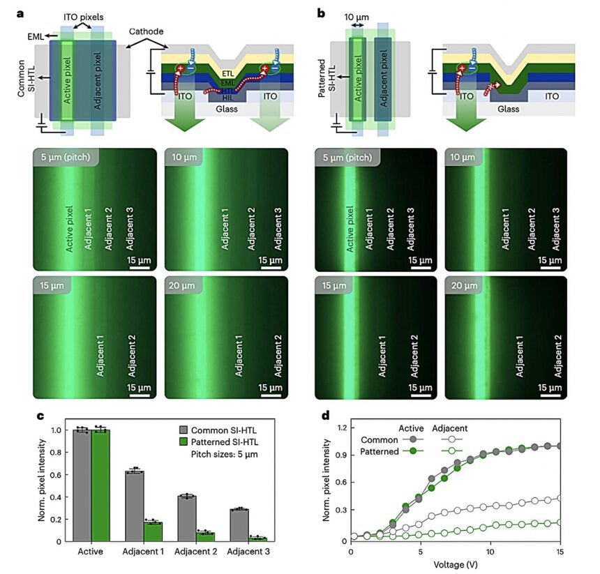
“Excessive-density shows are required for the event of digital and augmented actuality units,” Hyukmin Kweon, Seonkwon Kim and their colleagues wrote of their paper. “Nevertheless, growing the pixel decision can result in larger electrical pixel crosstalk, primarily as a consequence of a shared gap transport layer. We present {that a} silicone-integrated small-molecule gap transport layer might be patterned on the wafer scale with microlithography to mitigate electrical pixel crosstalk.”
Utilizing microlithography, the researchers created the SI-HTL layer and built-in it in OLEDs. They then created micro-patterned OLED arrays and examined their efficiency in a sequence of checks.
Notably, they discovered that the opening transport layer they created exhibited an improved efficiency. The prototype show they created was discovered to allow exceptional pixel resolutions, whereas additionally retaining a great power effectivity.
“With this strategy, we create high-fidelity micro-pattern arrays with a decision of as much as 10,062 pixels per inch on a six-inch wafer,” wrote Kweon, Kim and their colleagues. “The silicone-integrated small-molecule gap transport layer can successfully modulate cost steadiness inside the emission layers, bettering the luminance traits of natural light-emitting diodes.
“We additionally present that natural light-emitting diodes built-in with micro-patterned silicone-integrated small-molecule gap transport layers have a diminished electrical pixel crosstalk in contrast with natural light-emitting diodes with a typical gap transport layer.”
This latest research by Kweon, Kim and their colleagues opens new prospects for the event of high-definition OLED shows that additionally exhibit glorious energy-efficiencies. These shows could possibly be built-in into a variety of digital units, together with digital actuality (VR) or augmented actuality (AR) headsets, good glasses, wearable applied sciences, good telephones, and lots of different electronics.
Extra data:
Hyukmin Kweon et al, Microlithography of gap transport layers for high-resolution natural light-emitting diodes with diminished electrical crosstalk, Nature Electronics (2025). DOI: 10.1038/s41928-024-01327-5
© 2025 Science X Community
Quotation:
Excessive-definition natural LED microdisplays with diminished electrical crosstalk might improve VR and AR experiences (2025, February 7)
retrieved 8 February 2025
from https://techxplore.com/information/2025-02-high-definition-microdisplays-electrical-crosstalk.html
This doc is topic to copyright. Other than any truthful dealing for the aim of personal research or analysis, no
half could also be reproduced with out the written permission. The content material is offered for data functions solely.