Hafnium oxide (HfO2) has attracted consideration as a promising materials for ultrathin semiconductors and different microelectronic gadgets. The robust ionic bond between hafnium and oxygen atoms in HfO2 provides it a excessive dielectric fixed, superior thermal stability, and a large band hole.
Notably, these properties may be maintained even on the atomic scale. In the meantime, these properties additionally pose challenges in reaching extremely exact and clean etching of HfO2 movies.
Now, a gaggle of researchers from Japan and Taiwan has efficiently etched HfO2 movies with atomic-level precision, smoothness, and uniformity with out using halogen-based gases.
Halogen-based gases, containing fluorine and/or chlorine, are generally utilized in plasma-enhanced atomic-layer etching (ALE) strategies for HfO2 and most different supplies. Nevertheless, these gases may be extremely poisonous and will act as greenhouse gases. Due to this fact, eliminating their use within the etching strategies might additionally contribute to sustainable manufacturing.
This achievement was printed within the journal Small Science.
As semiconductor gadgets advance, the important dimensions of their circuits are required to shrink to only a few nanometers. HfO2 is a powerful candidate for functions in such next-generation semiconductor gadgets, together with ultrathin gate insulators in 2D material-based field-emission transistors and superior nonvolatile reminiscence gadgets.
The plasma-enhanced ALE technique is commonly used for the anisotropic etching of HfO2. This technique makes use of energetic species, normally low-energy ions, to offer the power wanted to take away floor atoms from supplies by forming risky merchandise.
“Standard plasma-enhanced ALE strategies for HfO2 usually depend on a mixture of bodily and chemical etching through halogen-based gases and high-energy ion bombardment to facilitate the removing of nonvolatile halides,” defined Shih-Nan Hsiao, a professor at Nagoya College and the examine’s lead creator.
“Nevertheless, the byproducts generated by means of bodily sputtering usually have low volatility, inflicting them to stick to the chamber partitions and have sidewalls. This might impair the efficiency of digital gadgets.”
To beat this downside, a analysis group led by Professors Hsiao and Masaru Hori from the Heart for Low-temperature Plasma Sciences at Nagoya College in Japan collaborated with researchers from Ming Chi College of Expertise in Taiwan. They aimed to develop a brand new technique for etching HfO2 movies that may produce clean and uniform surfaces, together with constant etched depths by means of anisotropic etching.
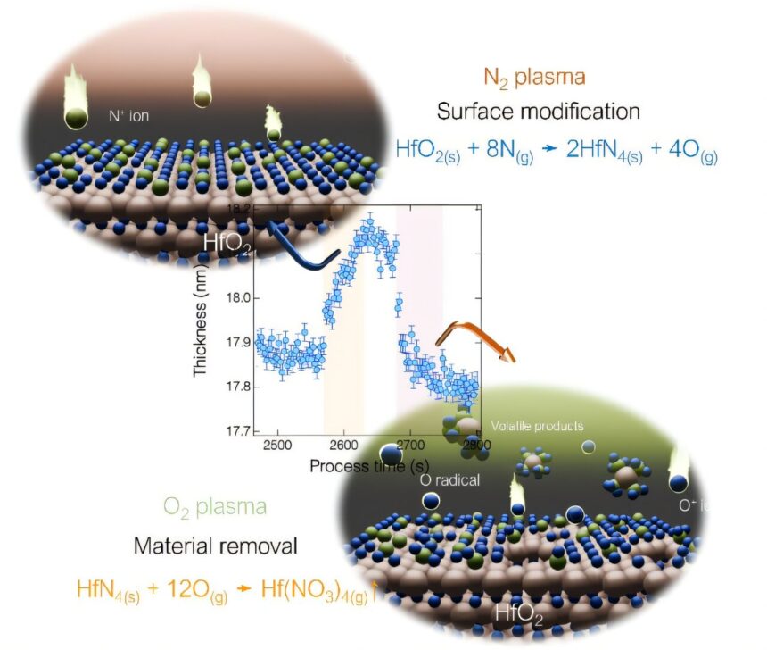
Researchers used a low-pressure, high-density plasma era system to irradiate HfO2 movies with N2 and O2 plasmas alternately.
In the course of the first half-cycle, N+ ions bombarded the HfO2 floor with an utilized bias voltage, resulting in the bonding of nitrogen with the HfO2. Subsequently, the HfO2 movies had been handled with an O2 plasma with out an utilized bias voltage. This process successfully eradicated the nitrogen-bonded floor layer by means of a self-limiting response.
Making use of radio-frequency energy to the underside electrode adjusted the power of the N+ ion. This adjustment led to an etch depth per cycle between 0.023 and 0.107 nm/cycle.
The researchers additionally analyzed the underlying floor response mechanism utilizing in situ strategies, particularly attenuated whole reflection Fourier remodel infrared spectroscopy and X-ray photoelectron spectroscopy.
This evaluation revealed a constant formation of Hf-N bonds by means of a ligand change mechanism. Throughout this course of, nitrogen atoms changed floor oxygen atoms when the pattern was uncovered to N2 plasma. Throughout the next half-cycle with O2 plasma, these bonds decomposed into risky byproducts.
Moreover, this cyclic etching approach successfully smoothed the HfO2 floor. After 20 cycles, the floor roughness was decreased by 60%.
Hsiao concluded, “We now have efficiently achieved halogen-free atomic-layer etching of HfO2 movie at room temperature for the primary time on this planet. Eliminating using halogen gases helps cut back environmental impacts.
“Performing the etching course of at room temperature saves power and simplifies the process, resulting in decrease manufacturing prices. Moreover, this course of is clear and eliminates response byproducts. Our work might subsequently contribute to sustainable manufacturing.”
Extra info:
Shih‐Nan Hsiao et al, Halogen‐Free Anisotropic Atomic‐Layer Etching of HfO2 at Room Temperature, Small Science (2025). DOI: 10.1002/smsc.202500251
Quotation:
Halogen-free plasma approach achieves atomic-level etching of hafnium oxide for next-gen semiconductors (2025, September 9)
retrieved 9 September 2025
from https://techxplore.com/information/2025-09-halogen-free-plasma-technique-atomic.html
This doc is topic to copyright. Other than any honest dealing for the aim of personal examine or analysis, no
half could also be reproduced with out the written permission. The content material is supplied for info functions solely.