To additional cut back the scale of digital gadgets, whereas additionally bettering their efficiency and power effectivity, electronics engineers have been making an attempt to establish various supplies that outperform silicon and different standard semiconductors. Two-dimensional (2D) semiconductors, supplies which are only a few atoms thick and have a tunable electrical conductivity, are among the many most promising candidates for the fabrication of smaller and higher performing gadgets.
Previous research confirmed that these supplies may very well be used to manufacture miniaturized transistors, digital elements that amplify or swap electrical indicators, notably field-effect transistors (FETs). These are transistors that management the movement {of electrical} present utilizing an electrical subject.
To reliably function, nonetheless, FETs additionally have to combine an insulating layer that separates the so-called gate electrode (i.e., the terminal regulating the movement of present) from the channel (i.e., the pathway via which electrical present flows). To allow higher management over the gate, this insulating layer, referred to as a gate dielectric, ought to have a excessive dielectric fixed (κ), or in different phrases, it ought to successfully retailer electrical power.
Sadly, reliably integrating 2D semiconductors with high-κ insulators has to this point proved tough. This, together with different technical challenges, is presently stopping the widespread adoption of FETs primarily based on 2D supplies.
Researchers at Nationwide Chung Hsing, Kansai College, Nationwide Cheng Kung College and different institutes lately launched a brand new technique to reliably use freestanding membranes made from hafnium zirconium oxide (Hf0.5Zr0.5O2; HZO) as high- κ gate dielectrics in 2D FETs. Their proposed method, outlined in a paper published in Nature Electronics, opens new prospects for the creation of small and energy-efficient transistors, in addition to extremely performing logic-in-memory methods.
“2D semiconductors may very well be used as a channel materials in miniaturized transistors with excessive gate management,” wrote Che-Yi Lin, Bo-Cia Chen and their colleagues of their paper. “Nevertheless, the shortage of insulators which are each suitable with two-dimensional supplies and appropriate for integration into a totally scalable course of movement limits improvement. We present that freestanding Hf0.5Zr0.5O2 or HZO membranes could be built-in with two-dimensional semiconductors as a high-κ dielectric.”
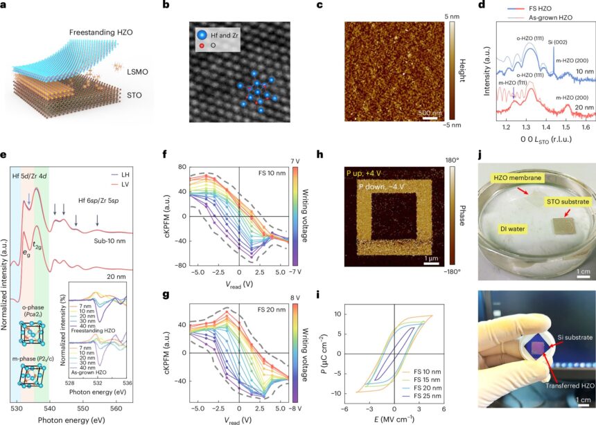
As a part of their research, the researchers first created freestanding HZO-based membranes. On this context, the time period ‘freestanding’ implies that the membranes don’t have to be immediately grown on a substrate, however can as a substitute be transferred onto it independently.
“The HZO membranes could be diversified in thickness from 5 to 40 nm, and be transferred onto molybdenum disulfide (MoS2) to create the top-gate dielectric in field-effect transistors,” wrote the authors.
“A 20-nm-thick HZO membrane displays a dielectric fixed of 20.6 ± 0.5 and a leakage present (at 1 MV cm−1) of below 2.6 × 10⁻⁶ A cm−2, under the necessities of the Worldwide Know-how Roadmap for Semiconductors, in addition to typical ferroelectric conduct. The MoS2 transistors with HZO dielectric exhibit an on/off ratio of 109 and a subthreshold swing under 60 mV dec−1 throughout 4 orders of present.”
To reveal the potential of their fabrication technique, the researchers used it to efficiently create quite a lot of digital elements. The ensuing gadgets had been discovered to carry out remarkably nicely, outperforming many 2D semiconductor-based digital elements developed prior to now.
“We use the transistors to create an inverter, logic gates and a 1-bit full adder circuit,” wrote the authors. “We additionally create a MoS2 transistor with a channel size of 13 nm, which displays an on/off ratio of over 108 and a subthreshold swing of 70 mV dec−1.”
This current research by Che-Yi Lin, Bo-Cia Chen and their colleagues, and the brand new method they launched, may contribute to the development of transistors and different gadgets primarily based on 2D semiconductors. As a part of their future research, the researchers may refine their method, whereas additionally additional assessing its reliability and compatibility with present electronics manufacturing processes.
Written for you by our writer Ingrid Fadelli,
edited by Gaby Clark, and fact-checked and reviewed by Robert Egan—this text is the results of cautious human work. We depend on readers such as you to maintain impartial science journalism alive.
If this reporting issues to you,
please contemplate a donation (particularly month-to-month).
You may get an ad-free account as a thank-you.
Extra data:
Che-Yi Lin et al, Integration of freestanding hafnium zirconium oxide membranes into two-dimensional transistors as a high-κ ferroelectric dielectric, Nature Electronics (2025). DOI: 10.1038/s41928-025-01398-y.
© 2025 Science X Community
Quotation:
Freestanding hafnium zirconium oxide membranes can allow superior 2D transistors (2025, July 31)
retrieved 2 August 2025
from https://techxplore.com/information/2025-07-freestanding-hafnium-zirconium-oxide-membranes.html
This doc is topic to copyright. Aside from any truthful dealing for the aim of personal research or analysis, no
half could also be reproduced with out the written permission. The content material is offered for data functions solely.