The European Fee has authorised a €1.3bn funding initiative to assist the institution of a semiconductor superior packaging and testing facility in Novara, Italy.
The initiative, led by Silicon Field, is a part of a broader technique to strengthen Europe’s semiconductor manufacturing business.
This transfer aligns with the European Chips Act and the European Commission’s 2024-2029 Political Guidelines, aiming to reinforce the EU’s safety of provide and technological autonomy in a essential sector.
The event follows the latest main information of €5bn EU funding to assist a semiconductor manufacturing plant in Dresden, Germany.
Teresa Ribera, Govt Vice-President for Clear, Simply and Aggressive Transition, commented: “The €1.3bn Italian measure authorised immediately helps a first-of-a-kind facility for superior packaging of chips.
“It ensures that key gamers within the telecommunications, automotive, or client electronics sectors have entry to high-performant, dependable and energy-efficient chips.
“This can assist our digital and inexperienced transitions and assist create high-skilled employment. On the similar time, we be sure that potential distortions of competitors are restricted.”
Boosting Europe’s semiconductor independence
Semiconductors are integral to fashionable know-how, powering gadgets and programs starting from smartphones to superior automobiles.
Current international provide chain disruptions have underscored the pressing want for Europe to extend its manufacturing capability and cut back reliance on exterior suppliers.
The European Chips Act, launched in February 2022 and enacted in September 2023, is a complete legislative framework designed to handle these challenges.
It promotes investments in semiconductor infrastructure, safeguards the EU’s provide chain resilience, and helps technological innovation.
The approval of Silicon Field’s semiconductor superior packaging venture marks the fifth main choice beneath the Chips Act, demonstrating the EU’s dedication to reinforcing its semiconductor ecosystem.
This new facility is anticipated to play a pivotal position in advancing Europe’s capabilities in semiconductor packaging and testing applied sciences.
Inside Italy’s semiconductor packaging venture
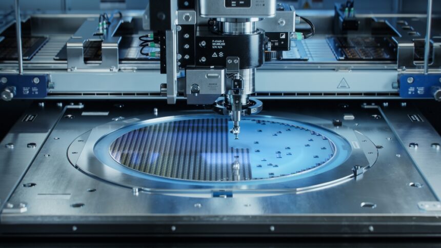
The €1.3bn in direct funding will complement Silicon Field’s €3.2bn funding within the new facility. This superior plant will give attention to semiconductor superior packaging, a course of that integrates a number of chips, often called ‘chiplets,’ right into a single bundle.
This innovation enhances the chips’ efficiency and vitality effectivity, making them simpler for a spread of functions.
In contrast to conventional wafer-level packaging strategies, the Novara facility will make use of panel-level packaging mixed with modern 3D integration methods.
This method will allow the manufacturing of extremely environment friendly multi-chip modules. As soon as totally operational, the power is anticipated to course of roughly 10,000 panels per week, with full capability anticipated by 2033.
The plant will perform essential phases of semiconductor manufacturing, together with chip meeting, superior packaging, and complete testing.
These capabilities are anticipated to considerably improve Europe’s semiconductor manufacturing capability whereas fostering innovation within the growth of next-generation applied sciences
Advantages and long-term commitments
The Silicon Field venture is anticipated to ship far-reaching advantages to the EU’s semiconductor ecosystem.
The brand new facility will strengthen Europe’s semiconductor worth chain by offering superior packaging options that create alternatives for collaboration and progress throughout the business.
Silicon Field has additionally dedicated to advancing the event of cutting-edge packaging applied sciences, positioning the EU as a worldwide chief on this discipline.
Moreover, the venture is designed to handle provide chain vulnerabilities by prioritising essential orders throughout instances of scarcity, as mandated by the European Chips Act.
Along with these industrial advantages, the initiative will contribute to workforce growth. Silicon Field will set up complete coaching and academic programmes to construct a pool of extremely expert professionals. This effort will guarantee a sustainable pipeline of expertise to assist Europe’s increasing semiconductor business.
A landmark transfer towards semiconductor sovereignty
By supporting the institution of a state-of-the-art semiconductor superior packaging facility, the EU is lowering its dependency on exterior suppliers whereas fostering innovation and financial progress.
The Novara facility is poised to grow to be a cornerstone of Europe’s semiconductor technique, driving the event of superior applied sciences and guaranteeing provide chain resilience.
Because the EU continues to strengthen its place on this important sector, it’s laying the groundwork for long-term competitiveness and technological management in a quickly evolving international panorama.