Friday, 27 Mar 2026
Subscribe
logo
  • Global
  • AI
  • Cloud Computing
  • Edge Computing
  • Security
  • Investment
  • Sustainability
  • More
    • Colocation
    • Quantum Computing
    • Regulation & Policy
    • Infrastructure
    • Power & Cooling
    • Design
    • Innovations
    • Blog
Font ResizerAa
Data Center NewsData Center News
Search
  • Global
  • AI
  • Cloud Computing
  • Edge Computing
  • Security
  • Investment
  • Sustainability
  • More
    • Colocation
    • Quantum Computing
    • Regulation & Policy
    • Infrastructure
    • Power & Cooling
    • Design
    • Innovations
    • Blog
Have an existing account? Sign In
Follow US
© 2022 Foxiz News Network. Ruby Design Company. All Rights Reserved.
Data Center News > Blog > Innovations > Creating compact near-sensor computing chips via 3D integration of 2D materials
Innovations

Creating compact near-sensor computing chips via 3D integration of 2D materials

Last updated: November 10, 2024 4:50 pm
Published November 10, 2024
Share
Creating compact near-sensor computing chips via 3D integration of 2D materials
SHARE
Characterization of 2D supplies and fabrication course of circulation for M3D integration. a, Optical picture of a 2-inch sapphire wafer with MOCVD-grown MoS2. Scale bar, 2.5 cm (1 inch) b, The corresponding Raman spectrum with the attribute E1 2g peak at 387 cm−1 and A1g peak at 404 cm−1. c, Optical picture of commercially bought monolayer graphene movie on a copper substrate. Scale bar, 40 mm. d, The corresponding Raman spectra obtained utilizing a 532 nm laser. e, Fabrication course of circulation of the 3D monolithic and heterogeneous integration of monolayer-MoS2- and graphene-based units. Credit score: Ghosh et al. (Nature Electronics, 2024).

Three-dimensional (3D) integration has opened new prospects for the event of denser circuits with extra interconnected digital elements. 3D integration approaches entail stacking a number of layers of digital circuits collectively, finally producing extra compact and environment friendly units.

These electronics fabrication methods can scale back each the scale and the facility consumption of electronics whereas additionally boosting their efficiency. An rising 3D integration method that has been discovered to be significantly promising is monolithic 3D (M3D) integration, which entails the development of transistors layer by layer on the identical substrate as an alternative of bonding particular person chips collectively.

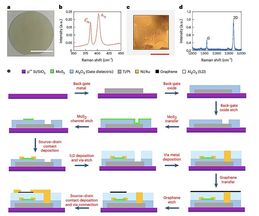
Researchers at Pennsylvania State College just lately developed extremely compact near-sensor computing chips through the heterogeneous M3D integration of two-dimensional (2D) supplies. Their paper, published in Nature Electronics, demonstrates the fabrication of those chips utilizing scalable methods which are suitable with present manufacturing processes.

“M3D integration is being more and more adopted by the semiconductor business as an alternative choice to conventional through-silicon through expertise, as a approach to improve the density of stacked, heterogenous digital elements,” Subir Ghosh, Yikai Zheng and their colleagues wrote of their paper. “M3D integration can even present transistor-level partitioning and materials heterogeneity. Nevertheless, there are few large-area demonstrations of M3D integration utilizing non-silicon supplies.”

As a part of their latest research, Ghosh, Zheng and their colleagues got down to develop a sensing and near-sensor computing chip based mostly on 2D electronics using an M3D integration technique. The chip they created integrates over 500 chemitransistors and over 500 memtransistors, with vertical interconnects (vias) which are 3 μm in dimension and at a 1 μm distance from one another.

See also  Boston Materials Raises $13.5M in Funding

“We report heterogeneous M3D integration of two-dimensional supplies utilizing a dense inter-via construction with an interconnect (I/O) density of 62,500 I/O per mm2,” Ghosh, Zheng and their colleagues wrote. “Our M3D stack consists of graphene-based chemisensors in tier 2 and molybdenum disulfide (MoS2) memtransistor-based programmable circuits in tier 1, with greater than 500 units in every tier. Our course of permits the bodily proximity between sensors and computing components to be decreased to 50 nm, offering decreased latency in near-sensor computing purposes.”

A key benefit of the M3D integration method employed by the researchers is that your complete fabrication course of takes place at temperatures underneath 200 °C. This implies it’s suitable with back-end-of-line integration processes presently used to manufacture semiconductor-based units.

As a part of their research, Ghosh, Zheng and their colleagues used the computing chip they developed for chemical codification. Particularly, they developed an alert system that might be used to determine and classify totally different chemical substances.

The chemitransistors within the workforce’s chip had been uncovered to sugar options with totally different concentrations and {the electrical} indicators they generated in response to those options had been recorded. Subsequently, memtransistors processed the indicators generated by the chemitransistors, changing them into analog and digital codes.

The findings of the workforce’s alert system demonstrations spotlight the potential of the brand new near-sensing computing chip for processing and classifying chemical substances. Sooner or later, their proposed fabrication method might be scaled as much as develop chips with a fair better variety of circuits and sensors, which might sort out extra superior classification duties.

See also  Embracing Moonshot Innovation in the AI revolution

Extra data:
Subir Ghosh et al, Monolithic and heterogeneous three-dimensional integration of two-dimensional supplies with high-density vias, Nature Electronics (2024). DOI: 10.1038/s41928-024-01251-8

© 2024 Science X Community

Quotation:
Creating compact near-sensor computing chips through 3D integration of 2D supplies (2024, November 10)
retrieved 10 November 2024
from https://techxplore.com/information/2024-11-compact-sensor-chips-3d-Second.html

This doc is topic to copyright. Other than any honest dealing for the aim of personal research or analysis, no
half could also be reproduced with out the written permission. The content material is supplied for data functions solely.


Source link

TAGGED: Chips, compact, computing, creating, Integration, materials, nearsensor
Share This Article
Twitter Email Copy Link Print
Previous Article Electricity demand for data centres in Europe could more than double by 2030 Electricity demand for data centres in Europe could more than double by 2030
Next Article Boston Materials Boston Materials Raises $13.5M in Funding
Leave a comment

Leave a Reply Cancel reply

Your email address will not be published. Required fields are marked *

Your Trusted Source for Accurate and Timely Updates!

Our commitment to accuracy, impartiality, and delivering breaking news as it happens has earned us the trust of a vast audience. Stay ahead with real-time updates on the latest events, trends.
FacebookLike
TwitterFollow
InstagramFollow
YoutubeSubscribe
LinkedInFollow
MediumFollow
- Advertisement -
Ad image

Popular Posts

DeepSeek-R1 reasoning models rival OpenAI in performance

DeepSeek has unveiled its first-generation DeepSeek-R1 and DeepSeek-R1-Zero fashions which might be designed to deal…

January 20, 2025

Blinq Raises $25M in Series A Funding

Blinq product picture Blinq, a Melbourne, Australia-based supplier of a digital enterprise card platform, raised…

May 8, 2025

Streamlining edge site management with GitOps: Empowering manufacturers in the digital era

By Kangwarn Chinthammit, Director, Know-how Product Supervisor, Software program Outlined Edge at Broadcom Trendy producers…

June 7, 2024

How to Raise Capital for Your New Business Venture

Being a budding entrepreneur comes with its fair proportion of difficulties, and one of the…

November 24, 2024

80 MW Blackpool data centre wins planning approval

A deliberate 80 MW knowledge centre at Peel Park on the outskirts of Blackpool has…

February 14, 2026

You Might Also Like

Fuelling defence goals with compound semiconductors from South Wales
Innovations

Fuelling defence goals with compound semiconductors

By saad
X-ray breakthrough enables real-time monitoring of electronic chips
Innovations

X-ray breakthrough enables real-time monitoring of electronic chips

By saad
AI could accurately deliver flood warnings in data-scarce regions
Innovations

AI could accurately deliver flood warnings in data-scarce regions

By saad
Innatera advances neuromorphic edge AI chips using Synopsys simulation tools
Edge Computing

Innatera advances neuromorphic edge AI chips using Synopsys simulation tools

By saad
Data Center News
Facebook Twitter Youtube Instagram Linkedin

About US

Data Center News: Stay informed on the pulse of data centers. Latest updates, tech trends, and industry insights—all in one place. Elevate your data infrastructure knowledge.

Top Categories
  • Global Market
  • Infrastructure
  • Innovations
  • Investments
Usefull Links
  • Home
  • Contact
  • Privacy Policy
  • Terms & Conditions

© 2024 – datacenternews.tech – All rights reserved

Welcome Back!

Sign in to your account

Lost your password?
We use cookies to ensure that we give you the best experience on our website. If you continue to use this site we will assume that you are happy with it.
You can revoke your consent any time using the Revoke consent button.