The machine that may make tomorrow’s AI chips doable has simply been declared prepared for mass manufacturing – and the clock for the trade’s subsequent leap has formally began. ASML, the Dutch firm that holds a worldwide monopoly on industrial excessive ultraviolet lithography gear, confirmed this week that its Excessive-NA EUV tools have crossed the brink from technically spectacular to genuinely production-ready.
The announcement was made solely to Reuters by ASML’s chief know-how officer Marco Pieters forward of a technical convention in San Jose.
Present-generation EUV machines are approaching the outer fringe of what they will do for superior AI chip manufacturing, that means the semiconductors powering massive language fashions and AI accelerators are bumping up towards a bodily ceiling. Excessive-NA EUV instruments are designed to interrupt by way of it, letting chipmakers print finer, denser circuit patterns in fewer steps. That interprets immediately into extra highly effective and environment friendly chips for AI workloads.
“I feel that it’s at an necessary level to take a look at the quantity of studying cycles which have occurred,” Pieters advised Reuters, referring to the amount of buyer testing the machines have now collected.
The numbers that matter
ASML’s case for readiness rests on three information factors it plans to launch publicly. The Excessive-NA EUV instruments have now processed 500,000 silicon wafers, achieved roughly 80% uptime – with a goal of 90% by year-end – and demonstrated imaging precision able to changing a number of standard patterning steps with a single Excessive-NA cross.
Collectively, Pieters stated, these figures sign that the instruments are prepared for producers to start qualification. The machines don’t come low cost. At roughly US$400 million per unit – double the price of the earlier EUV technology – they signify some of the costly items of capital gear in industrial historical past.
TSMC and Intel are among the many named early adopters.
A two-to-three-year runway
Technical readiness and manufacturing integration are two various things, and Pieters was cautious to separate them. Regardless of the milestone, full integration into high-volume manufacturing strains continues to be anticipated to take two to 3 years as chipmakers work by way of qualification and course of growth.
“Chipmakers have all of the data to qualify these instruments,” he stated – a vote of confidence within the trade’s capacity to maneuver, even when the timeline stays measured.
The subsequent technology of chip efficiency enhancements is on the horizon, not but in hand. However with ASML now saying the beginning gun has fired, the race to combine Excessive-NA EUV into manufacturing has formally begun.
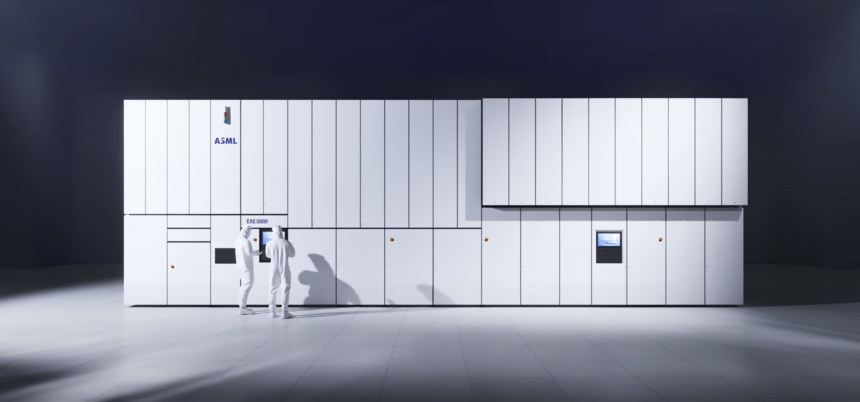
(Photograph by ASML)
See additionally: 2025’s AI chip wars: What enterprise leaders discovered about provide chain actuality
Wish to study extra about AI and massive information from trade leaders? Try AI & Big Data Expo happening in Amsterdam, California, and London. The great occasion is a part of TechEx and co-located with different main know-how occasions. Click on here for extra data.
AI Information is powered by TechForge Media. Discover different upcoming enterprise know-how occasions and webinars here.